Preparation and use of wireless reprogrammable multilateral optogenetic devices for behavioral neuroscience
Ferrona Lie, Yonggang Huang, John A. Rogers, Yiyuan Yang, Mingzheng Wu, Amy J. Wegener, Abraham Vázquez-Guardado, Andrew I. Efimov, Taoyi Wang, Yuhang Ma, Anthony Banks, Zhengwei Li, Zhaoqian Xie, Cameron H. Good, Yevgenia Kozorovitskiy


Extended
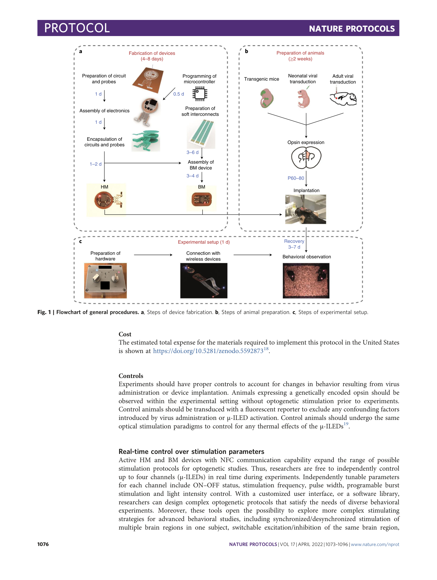
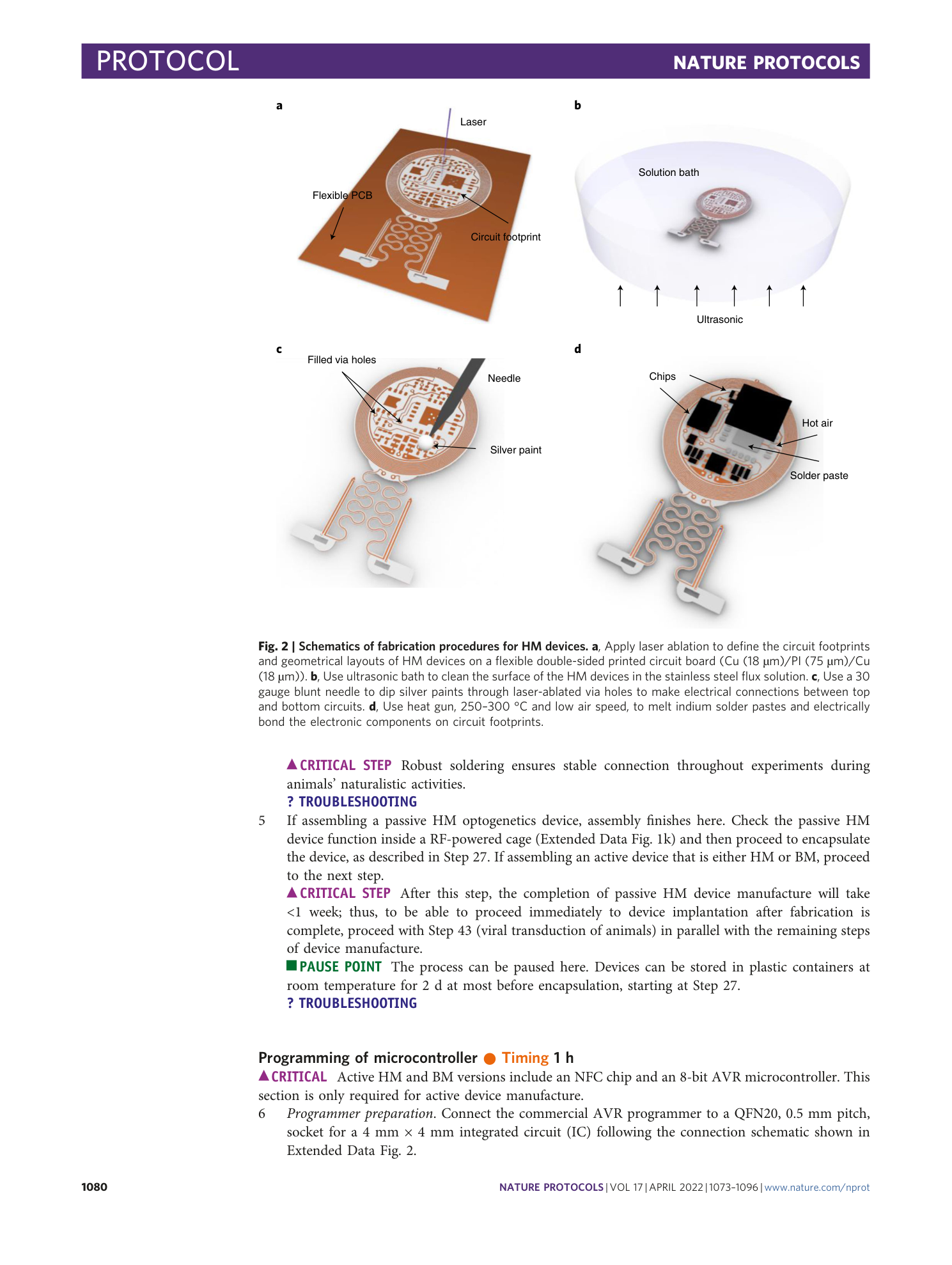
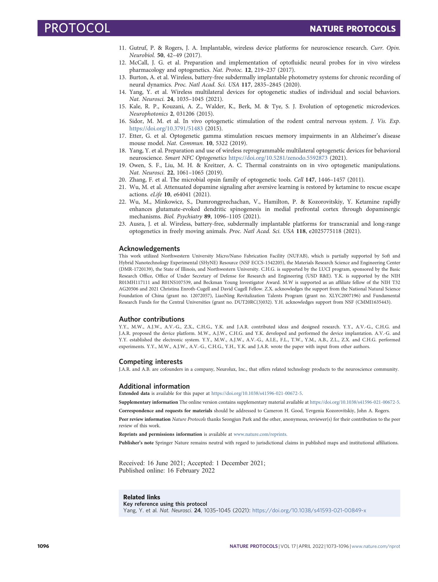
Extended Data Fig. 1 Preparation of the electronic module and probes.
a , Apply laser ablation to form the geometrical layouts and circuit footprints for electronic modules and probes. b , Use ultrasonic flux bath to clean the surfaces of modules and probes after laser ablation. c – e , Fill in laser-ablated via holes with liquid silver paint using a 30 gauge blunt needle to make electrical connections between top and bottom circuits: active HM device ( c ), BM module ( d ), passive HM device ( e ) and probes for BM devices ( f ). g – j , Solder electronic components on circuit footprint: active HM device ( g ), BM module ( h ), passive HM device ( i ), probes for BM devices ( j ). k – m , Device operation: passive HM device ( k ), active HM device ( l ), BM module ( m ).
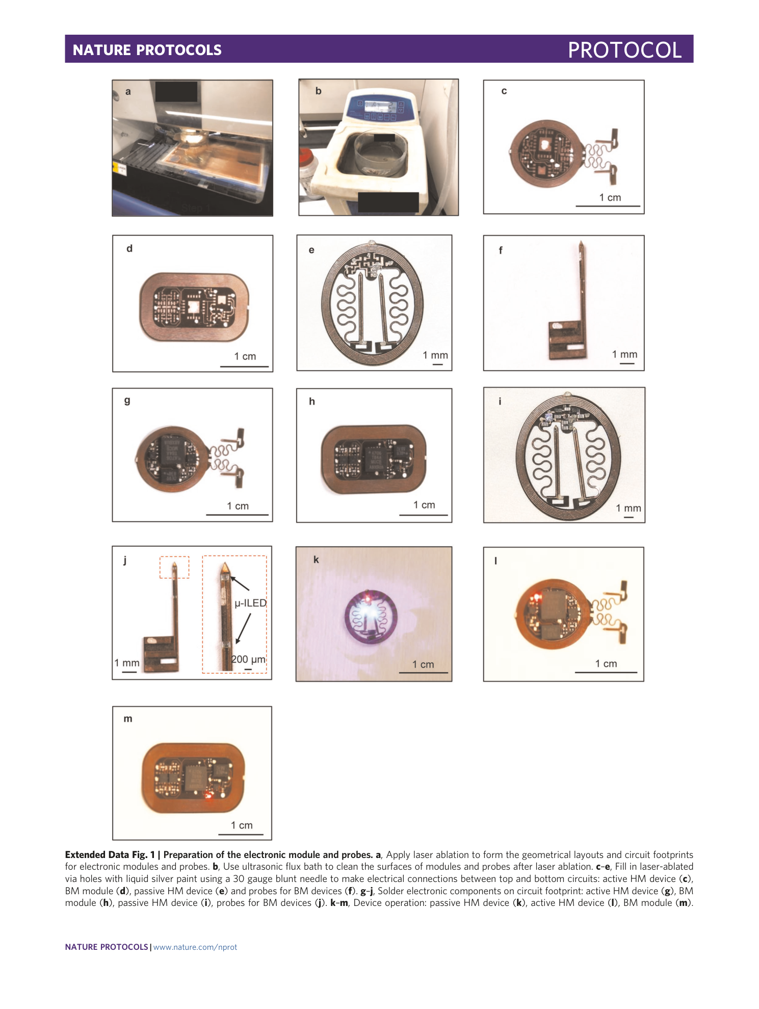
Extended Data Fig. 2 Attiny84 microcontroller programming using Arduino IDE.
The microcontroller is programmed using open-source Arduino software, commercial ISP programmer and QFN20 packaging adapter socket. (i) Open the microcontroller firmware using Arduino. Set the corresponding programming parameters. (ii) Connect the programmer to the computer. (iii) Mount the microcontroller chip onto the QFN20 socket and secure properly. Upload the firmware to the microcontroller.
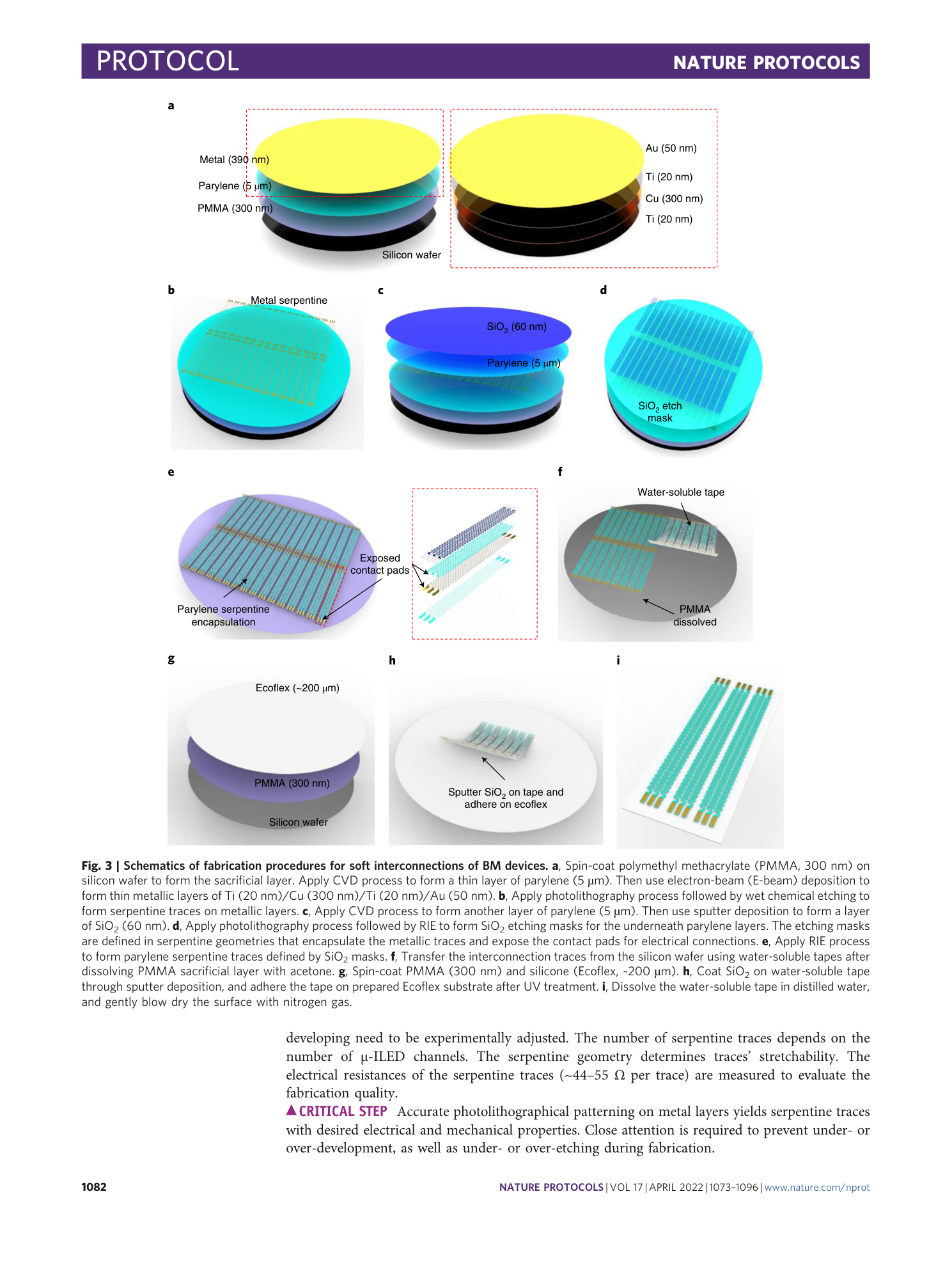
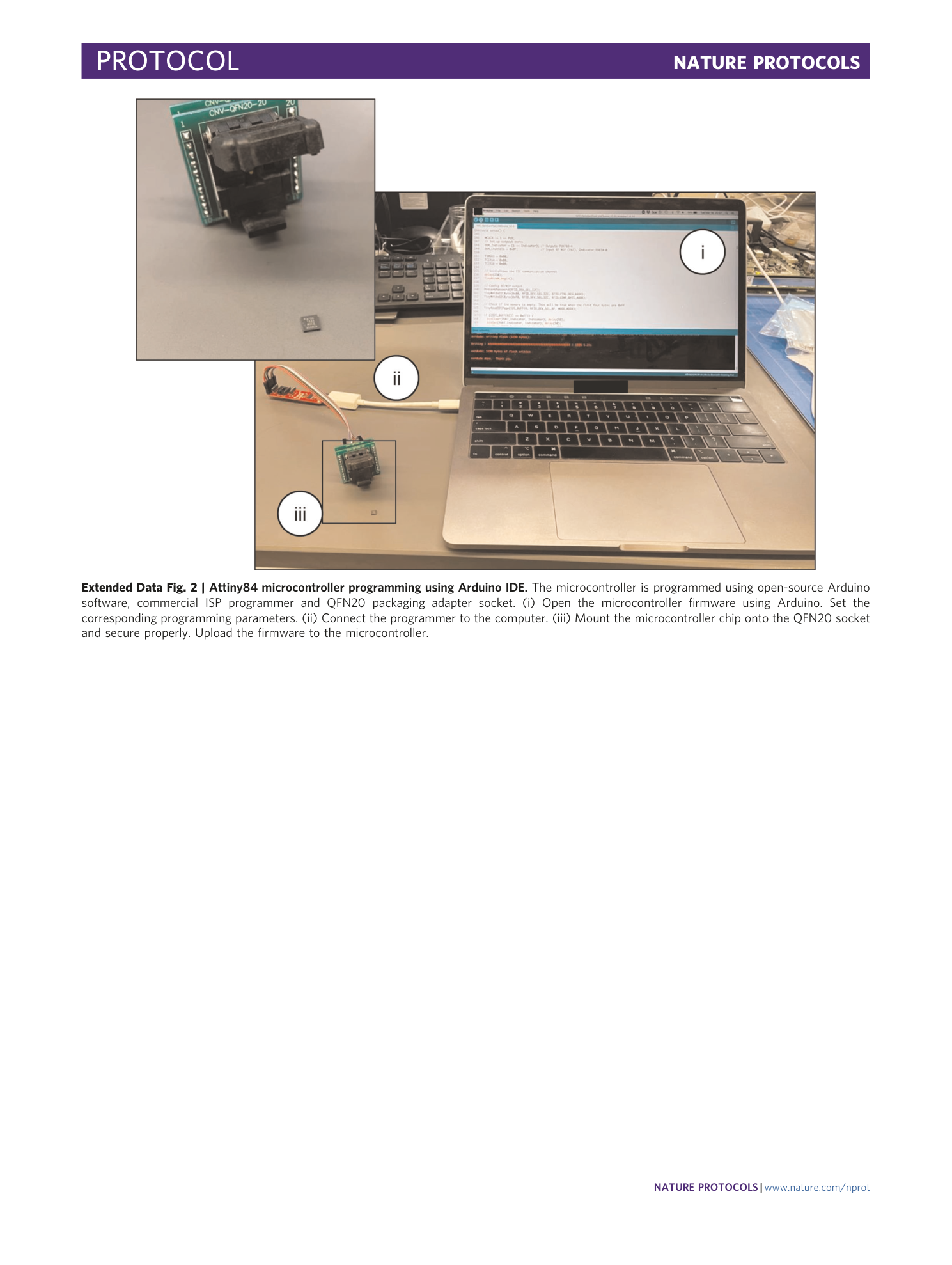
Extended Data Fig. 3 Preparation of soft interconnections for back-mounted devices.
a , Apply photolithographic method to define the serpentine geometries for metallic and SiO 2 layers. b , Use RIE to define the serpentine geometries of parylene encapsulation layers. The contact pads are exposed for electrical connections. c – f , Transfer printing process: cover the silicon wafer with a thin wipe (Kimtech) and another same-sized silicon wafer, and put it in an acetone bath heated by a hotplate at 80 °C for 120 min ( c ); use water-soluble tape to transfer the interconnection traces from silicon substrate ( d ); bond the interconnection traces on silicone substrate ( e ); dissolve tape in distilled water ( f ).
Extended Data Fig. 4 Preparation of tungsten strengthened probes.
a – c , Glue tungsten stiffeners on the active HM device ( a ), the passive HM device ( b ) and the probe for BM device ( c ). Scale bars, 5 mm.
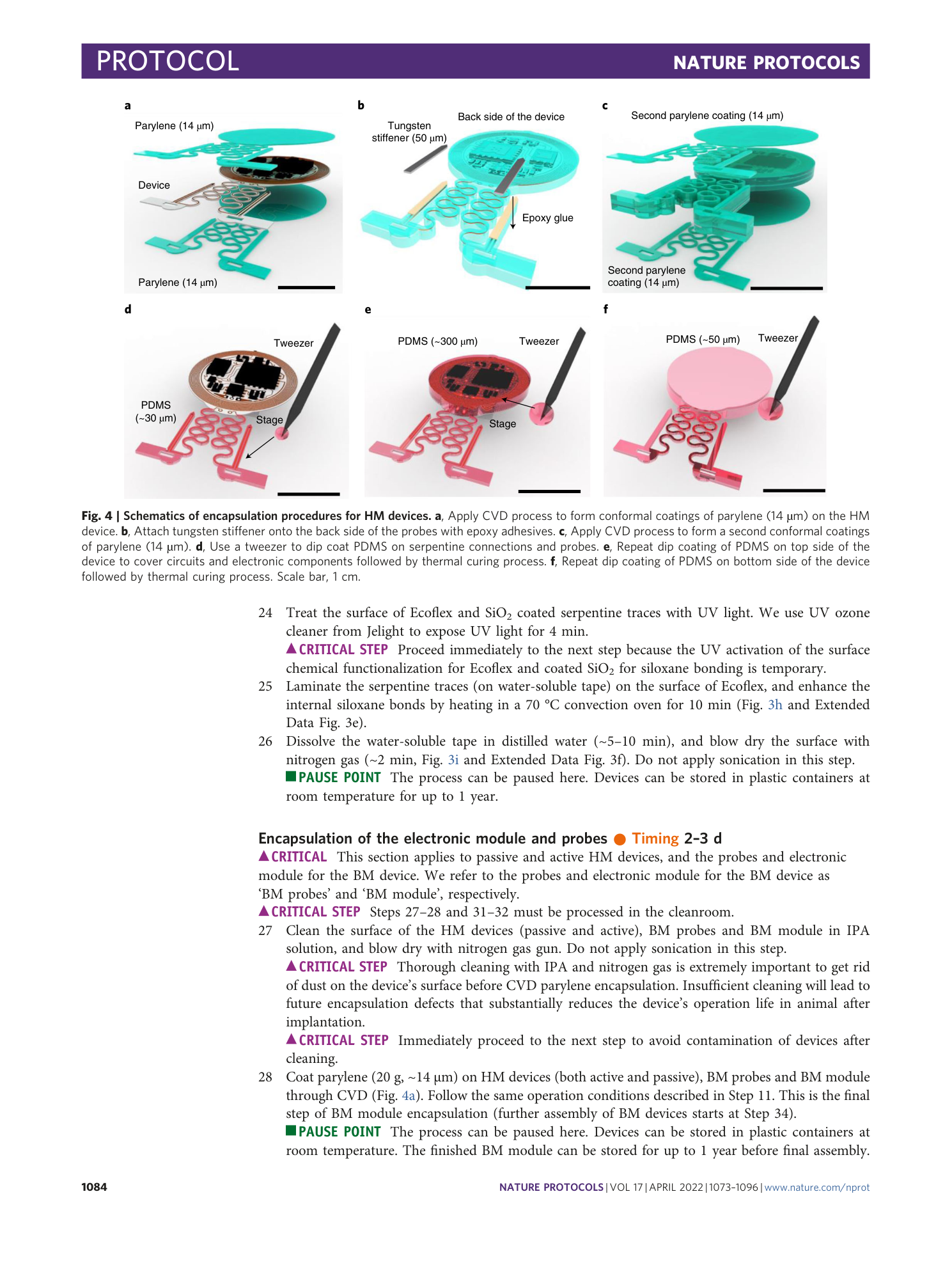
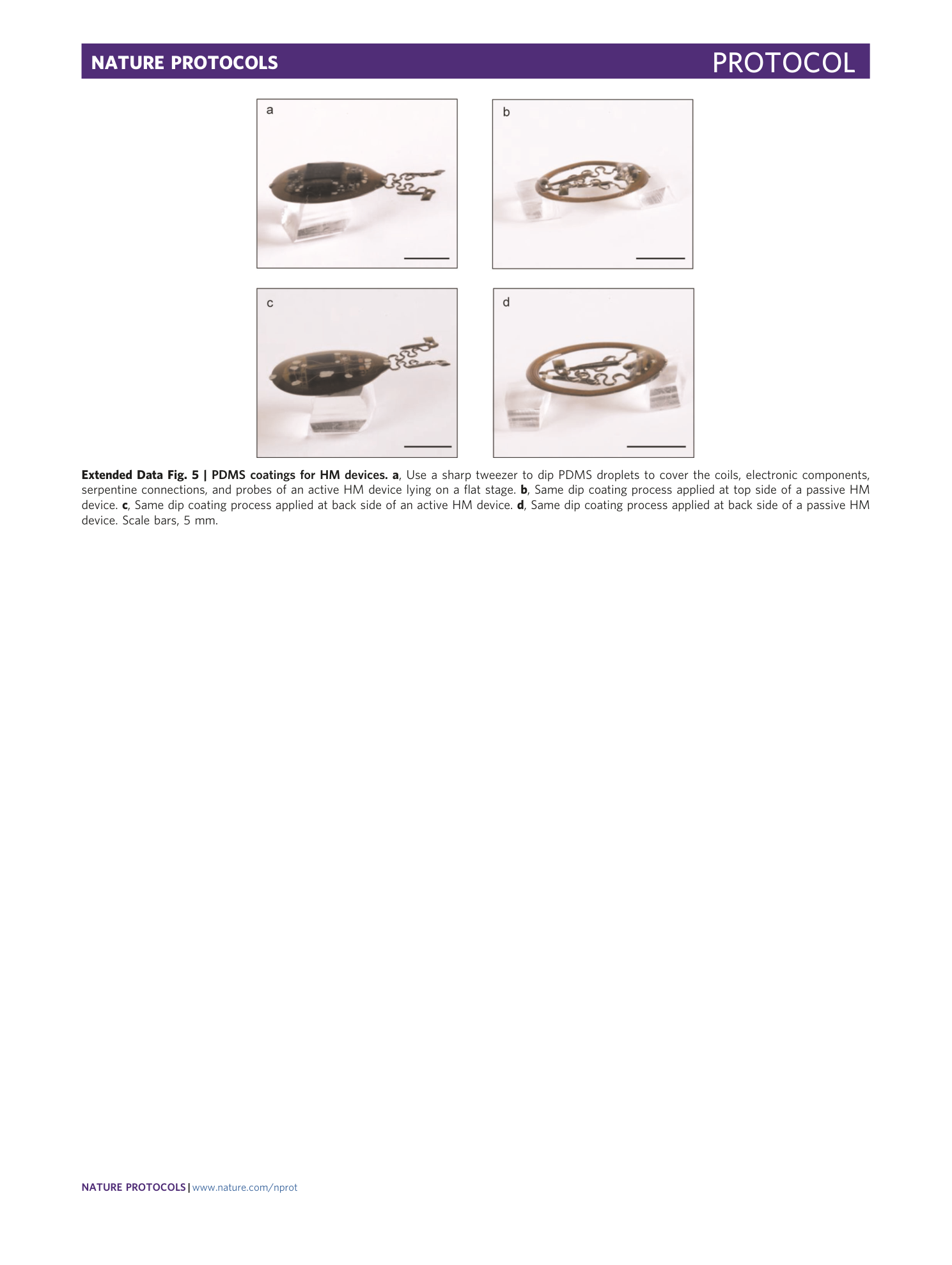
Extended Data Fig. 5 PDMS coatings for HM devices.
a , Use a sharp tweezer to dip PDMS droplets to cover the coils, electronic components, serpentine connections, and probes of an active HM device lying on a flat stage. b , Same dip coating process applied at top side of a passive HM device. c , Same dip coating process applied at back side of an active HM device. d , Same dip coating process applied at back side of a passive HM device. Scale bars, 5 mm.
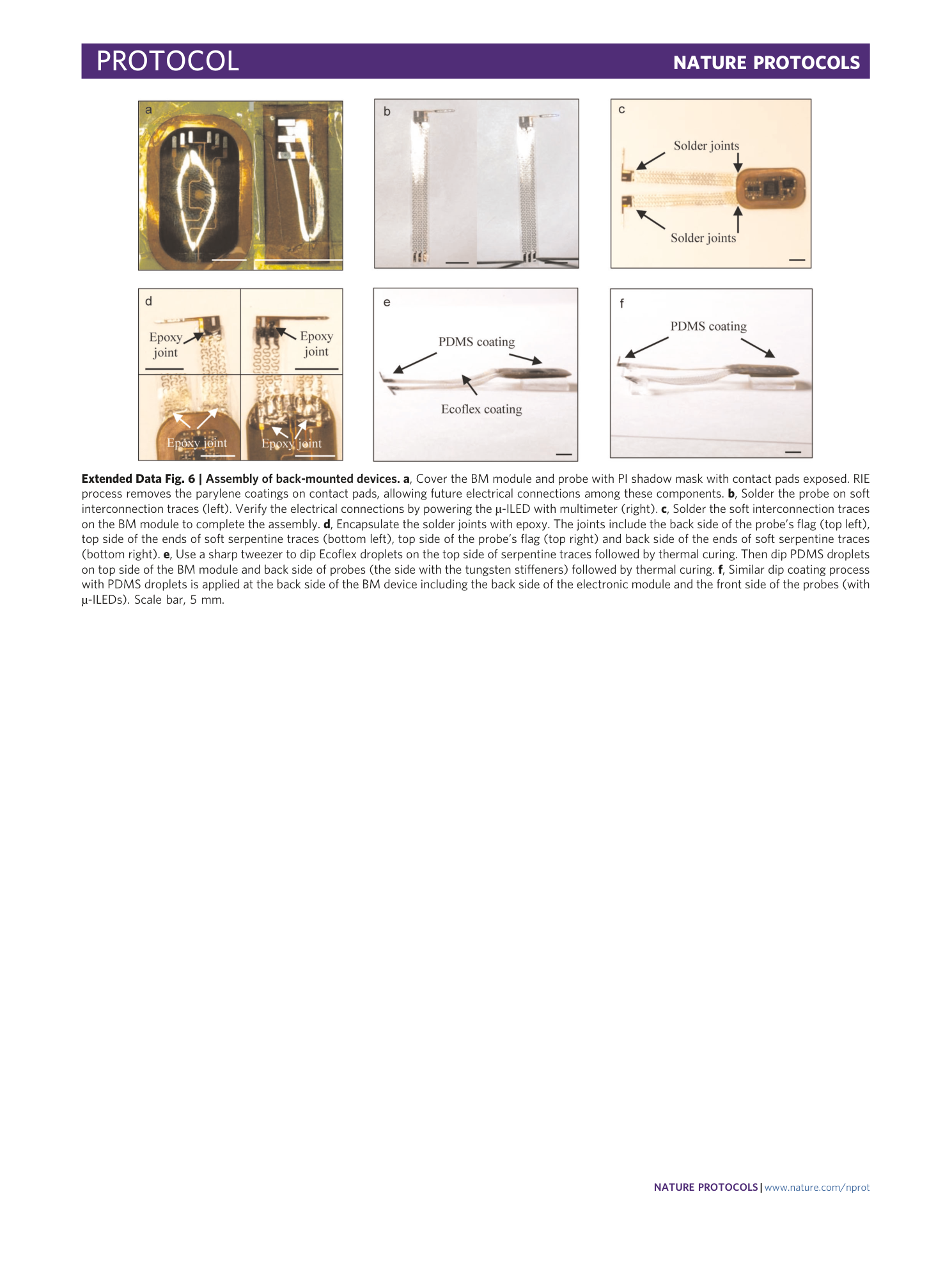
Extended Data Fig. 6 Assembly of back-mounted devices.
a , Cover the BM module and probe with PI shadow mask with contact pads exposed. RIE process removes the parylene coatings on contact pads, allowing future electrical connections among these components. b , Solder the probe on soft interconnection traces (left). Verify the electrical connections by powering the µ-ILED with multimeter (right). c , Solder the soft interconnection traces on the BM module to complete the assembly. d , Encapsulate the solder joints with epoxy. The joints include the back side of the probe’s flag (top left), top side of the ends of soft serpentine traces (bottom left), top side of the probe’s flag (top right) and back side of the ends of soft serpentine traces (bottom right). e , Use a sharp tweezer to dip Ecoflex droplets on the top side of serpentine traces followed by thermal curing. Then dip PDMS droplets on top side of the BM module and back side of probes (the side with the tungsten stiffeners) followed by thermal curing. f , Similar dip coating process with PDMS droplets is applied at the back side of the BM device including the back side of the electronic module and the front side of the probes (with µ-ILEDs). Scale bar, 5 mm.
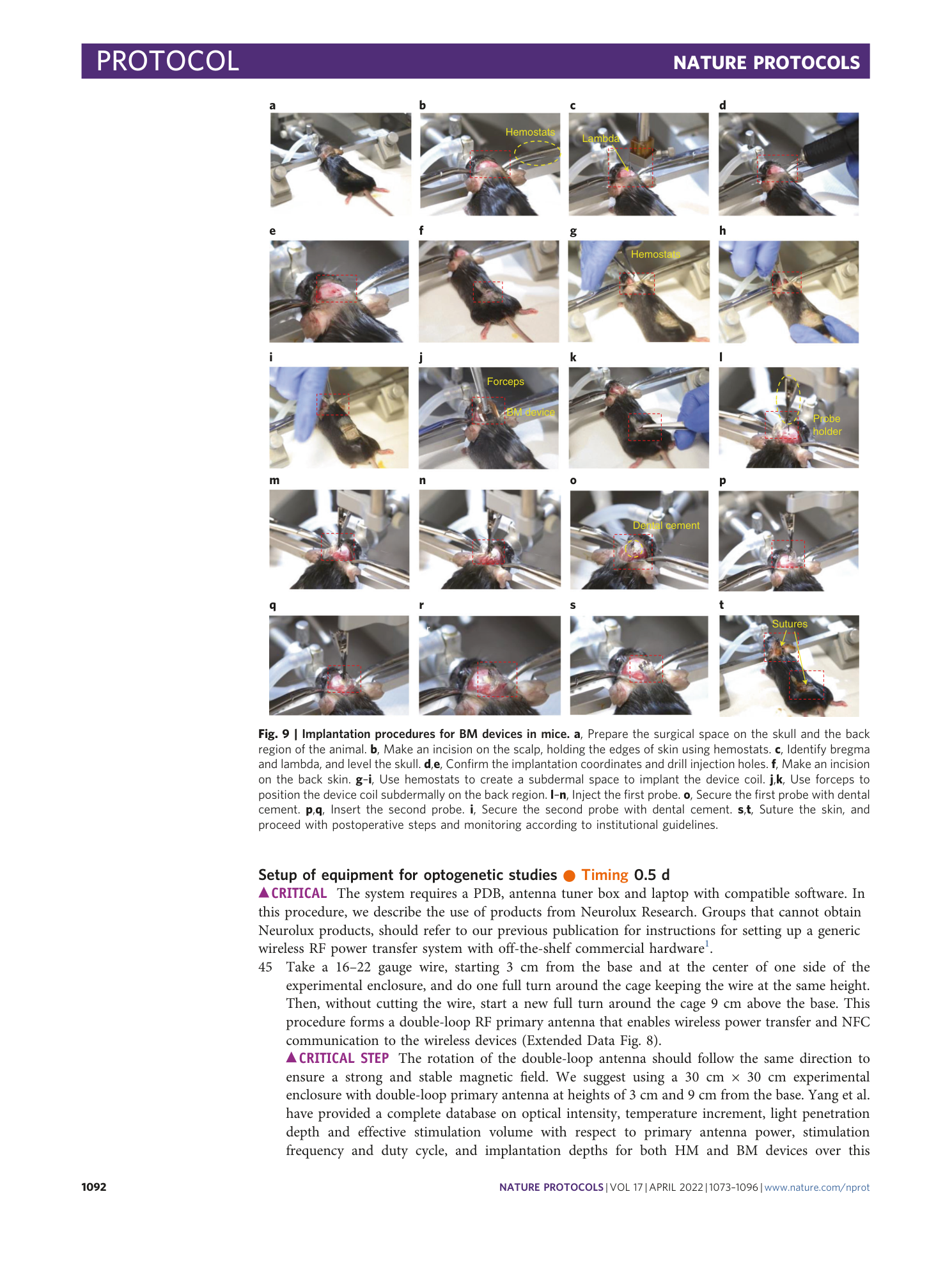
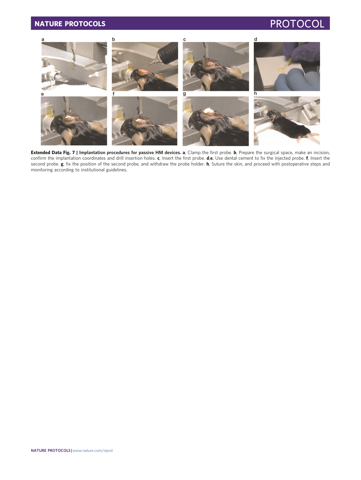
Extended Data Fig. 7 Implantation procedures for passive HM devices.
a , Clamp the first probe. b , Prepare the surgical space, make an incision, confirm the implantation coordinates and drill insertion holes. c , Insert the first probe. d , e , Use dental cement to fix the injected probe. f , Insert the second probe. g , fix the position of the second probe, and withdraw the probe holder. h , Suture the skin, and proceed with postoperative steps and monitoring according to institutional guidelines.
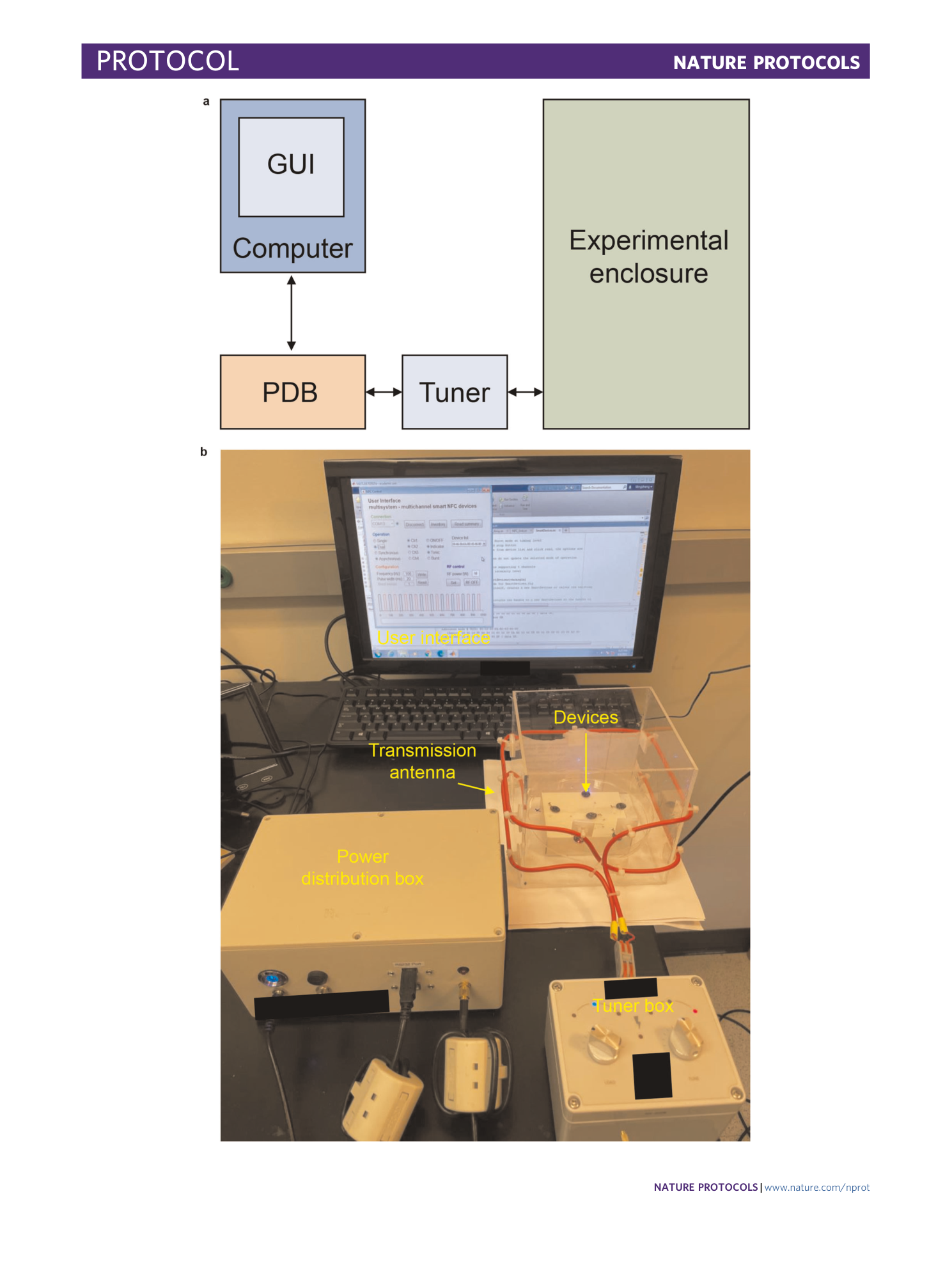
Extended Data Fig. 8 Experimental implementation.
a , Block diagram that indicates the implementation of the typical wireless optogenetics system. The graphic user interface (GUI) is hosted on a computer and interfaces with the power distribution controller (PDB) via serial interface. The PDB box drives radio frequency power at 13.56 MHz to the transmitting antenna on the experimental enclosure and transfers wireless power to the receiving antennae on the NFC devices. The impedance of the transmission antenna is properly matched using an impedance tuner (Tuner). The PDB, besides providing RF power, also relays read/write commands instructed from the GUI to the NFC device as the basis of wireless control of the mode of operation of the implantable devices. b , Photograph of a typical experimental implementation showing the hardware described in a .
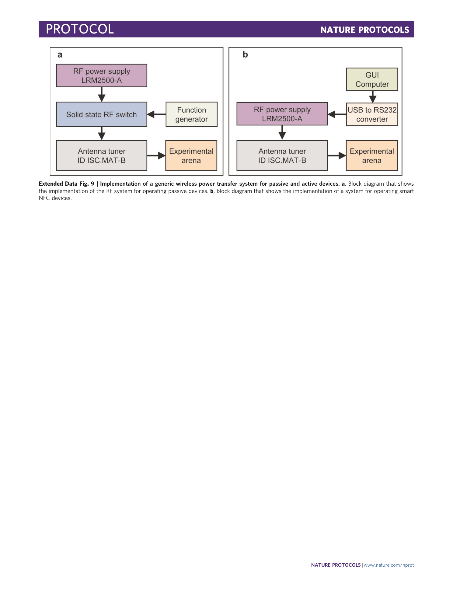
Extended Data Fig. 9 Implementation of a generic wireless power transfer system for passive and active devices.
a , Block diagram that shows the implementation of the RF system for operating passive devices. b , Block diagram that shows the implementation of a system for operating smart NFC devices.
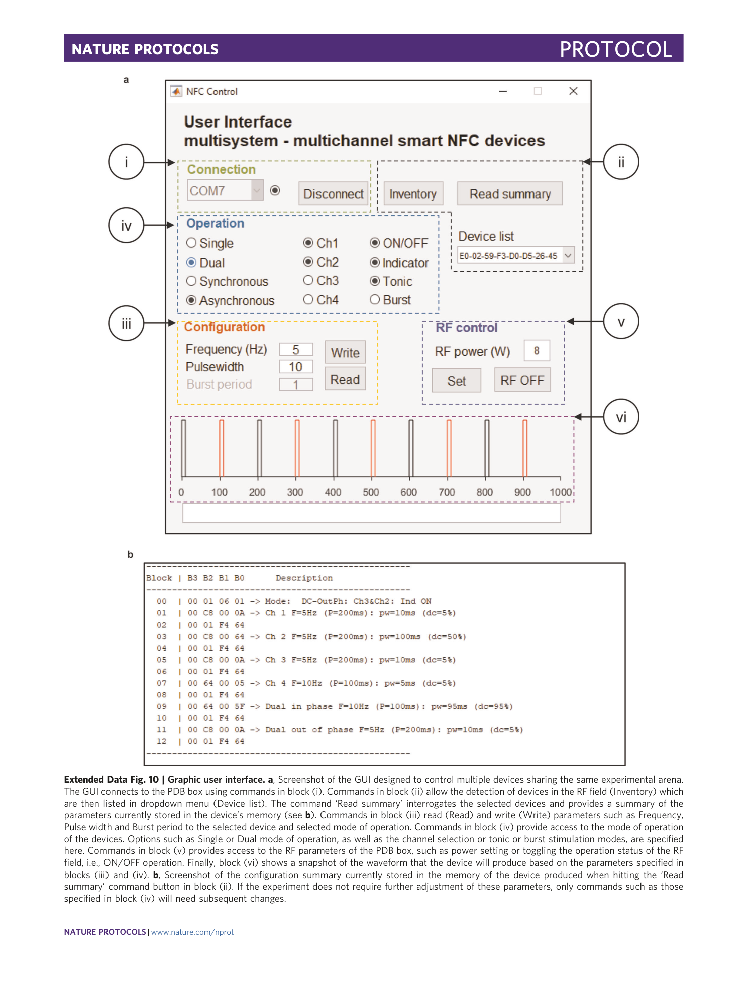
Extended Data Fig. 10 Graphic user interface.
a , Screenshot of the GUI designed to control multiple devices sharing the same experimental arena. The GUI connects to the PDB box using commands in block (i). Commands in block (ii) allow the detection of devices in the RF field (Inventory) which are then listed in dropdown menu (Device list). The command ‘Read summary’ interrogates the selected devices and provides a summary of the parameters currently stored in the device’s memory (see b ). Commands in block (iii) read (Read) and write (Write) parameters such as Frequency, Pulse width and Burst period to the selected device and selected mode of operation. Commands in block (iv) provide access to the mode of operation of the devices. Options such as Single or Dual mode of operation, as well as the channel selection or tonic or burst stimulation modes, are specified here. Commands in block (v) provides access to the RF parameters of the PDB box, such as power setting or toggling the operation status of the RF field, i.e., ON/OFF operation. Finally, block (vi) shows a snapshot of the waveform that the device will produce based on the parameters specified in blocks (iii) and (iv). b , Screenshot of the configuration summary currently stored in the memory of the device produced when hitting the ‘Read summary’ command button in block (ii). If the experiment does not require further adjustment of these parameters, only commands such as those specified in block (iv) will need subsequent changes.